Ncore’s Not Your Granny’s Coherent NoC (Network-on-Chip)
Things have evolved beyond all expectation since I designed my first ASIC.
March 27, 2024
At a Glance
- Arteris has announced the 3.6 release of the Ncore cache coherent NoC to support the latest Arm and RISC-V processors
- Pre-validated for use with Armv9 automotive cores, ISO 26262 certified Ncore offers a wide variety of automated FuSa features
I was just chatting with my chum Andy Nightingale, who is VP of Product Management and Marketing at Arteris IP.
What’s with the “IP” portion of the Arteris moniker? Well, in the context of system-on-chip (SoC) devices, the term intellectual property (IP) refers to the functional blocks that are combined to form the final device. The way this usually works is that most of the IPs—like processors, memory, controllers, peripherals, and communications functions—are sourced from trusted third-party vendors. This leaves the development team free to focus on integrating everything whilst also creating one or more of their own “secret sauce” IPs—like hardware accelerators or artificial intelligence (AI) engines—that will make this SoC stand proud in the crowd with respect to any competitive offerings.
In addition to providing chip-spanning network-on-chip (NoC) interconnect IP, which is used to connect the other IPs on the SoC together, Arteris IP also offers a suite of SoC integration automation and management tools, which greatly speeds the task of pulling all the IPs together and managing things like their hundreds-of-thousands (sometimes millions) of control and status registers (CSRs).
Andy was telling me that everyone at Arteris is currently bouncing off the walls with excitement because they’ve just announced the 3.6 release of their Ncore coherent Network-on-Chip (NoC).
In some ways, Arteris reminds me of the ~160-year-old company BASF, which is the largest chemical producer in the world. BASF used to have a famous series of commercials, the underlying theme of which was, “We don't make the products, we make them better." The point is that, outside of people in industry, the public was largely unaware of BASF’s existence, even though people were cognizant of the products created by other companies that were based on materials supplied by BASF. Similarly, outside of SoC architects, designers, and verification engineers, most people have never heard of Arteris, even though they have name recognition of the companies creating the SoCs that rely on Arteris NoC technology to make them work.
Just to put this into perspective, somewhere between 70% to 80% of SoCs used in advanced driver-assistance system (ADAS) automotive applications rely on Arteris NoC technology. Arteris also has a strong market presence and product offering in artificial intelligence (AI) and machine learning (ML) system IP. Their silicon-proven interconnect IP has been used in an eye-watering ~3.5 billion SoCs shipped to date, and this number is growing as I pen these words.
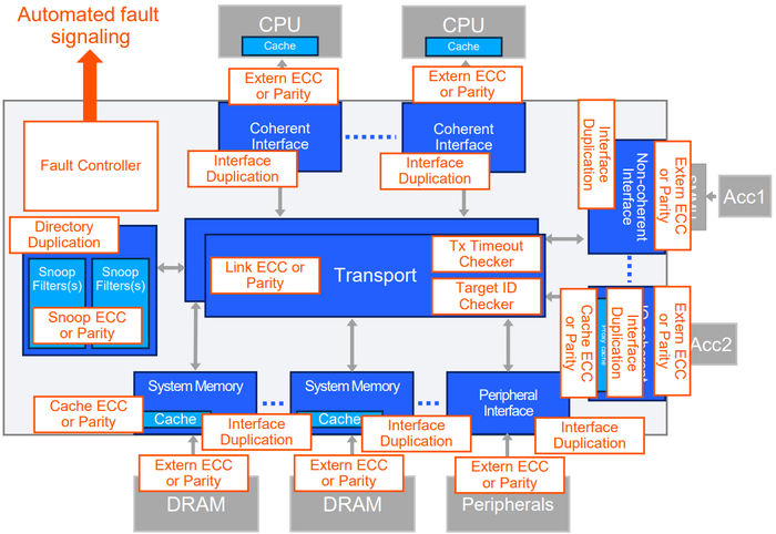
The ISO 26262 certified Ncore coherent NoC offers a wide variety of automated functional safety (FuSa) features. ARTERIS
Unless you are an SoC designer yourself, you may not be fully conversant with NoC concepts. Furthermore, even SoC designers may not be acquainted with the coherent NoC offerings from Arteris. So, let’s take a few moments to set the scene.
Way back in the mists of time when I designed my first application-specific integrated circuit (ASIC) circa 1980, we didn’t even have the concept of IPs (or computer-aided design tools, for that matter). I designed the entire device at the gate-and-register-level using pencil and paper. Functional verification involved other members of the team gathering around the table while you explained how your design performed its magic in the hope they would say, “Well, that looks like it will work.” Similarly, timing verification involved my identifying all the critical paths and then summing the delays on those paths by hand (I didn’t even have access to a simple 4-function calculator—those were reserved for executives who needed them to calculate their expense accounts and milage allowances—it’s a wonder I’m not bitter).
By the 1990s, vendors were offering unassuming IPs, and ASIC/SoC designers were connecting handfuls of these IPs using simple bus structures. By the early 2000s, IPs were much more complex, SoCs featured multiple initiator and target IPs, and designers moved to using many-to-many crossbar switch interconnect architectures. Circa the 2010s, when developers started to create SoCs containing hundreds of extremely large and enormously complex IPs, the crossbar concept became increasingly untenable due to silicon real estate utilization, routing congestion, and power consumption problems. The solution was found in the form of NoCs.
The easiest way to visualize a NoC is as an on-chip network servicing anywhere from a few to multiple hundreds of source (initiator) and destination (target) IPs. Some IPs can act as both initiators and targets, often at the same time. Different IPs from different vendors may employ different communication protocols, including APB, AHB, AXI, CHI, OCP, etc. Also, different IP interfaces may have different data widths running at different clock frequencies. The solution is to have agents (also known as “sockets”) that connect the IPs to the NoC. The agent associated with an initiator IP will packetize and serialize the data into a neutral format before handing it over to the NoC. The NoC will transport the packet to its destination (target) IP, where that IP’s agent (socket) will de-serialize, de-packetize, and present the data in the form (protocol, data width, clock frequency, etc.) required by that IP. Large numbers of packets can be “in-flight” through the NoC at the same time.
Designing a NoC is hard enough on a good day. It’s significantly more difficult to develop a coherent NoC. What do we mean by “coherent” in this context? Well, first we need to make sure we are all tap-dancing to the same skirl of the bagpipes with respect to our understanding of cache, by which we mean small, fast memories that are local to processor (and possibly accelerator) IP cores.
The idea here is that programs often perform multiple operations on the same data and identical operations on closely located data. It takes time and power for the SoC to access data from off-chip DRAM devices. Thus, when a SoC processor core requests a group of instructions and data from the main memory for the first time, a copy is stored in its local cache to be used for future operations. In fact, the core may have multiple levels of cache, each with its own copy of the same data. Consider a cluster of four processor cores, for example. A common scenario is for each core to have its own Level 1 (L1) cache, for pairs of cores to share L2 caches, and for all four cores to share an L3 cache.
The concept behind cache coherency is to ensure that everyone (IP-wise) knows who is holding the latest and greatest copy of each piece of data. A processor cluster is designed such that its cores automatically maintain cache coherency. The problem arises when there are multiple such clusters—along with accelerator IPs with their own caches—all of which need to maintain coherency. In this case, a coherent NoC must be used, where the NoC essentially implements an L4 cache, which is shared amongst all the other cores, and the NoC maintains coherency across the system.
Why don’t SoC design teams create their own NoCs? If the truth be told, some teams do attempt to do this, but it usually ends in tears. Why? Well, this will require multiple team members devoting a significant amount of time and effort to the NoC portion of the project. The amount of resources required will depend on the size and complexity of the project, but a conservative estimate for an advanced coherent NoC is 50 engineering years. That’s a lot of years. Especially when you realize that, in addition to debugging their own internally developed IPs (both in isolation and in the context of the rest of the SoC), the team will also end up spending an inordinate amount of time debugging their internally developed NoC.
There’s also the problem of keeping one’s own NoC up to date with evolving standards and protocols. Take Arm processors as just one example. Suppose a team has spent the past few years developing a NoC that, among other protocols, supports Arm’s CHI-B coherent interface. Sad to relate, this won’t work with the latest and greatest Armv9 Cortex automotive processor IPs, which support only CHI-E. “Oh dear,” I can imagine the team members saying (or words to that effect).
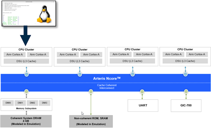
Ncore 3.6 has been pre-validated with Armv9 automotive cores. ARTERIS
All this explains why the folks at Arteris are beaming with joy about the 3.6 product release of their Ncore coherent NoC. Also, why the designers of SoCs from multiple markets—including automotive, communications. enterprise computing, industrial, and medical—are tap-dancing in the streets at the news.
In a crunchy nutshell, Ncore accelerates modern SoC designs and optimizes their performance by supporting heterogeneous processors and accelerators (e.g., Arm and RISC-V), multiple protocols (e.g., ACE, ACE-Lite, AXI, CHI-B, CHI-E), and multiple network topologies (e.g., ring, tree, mesh, torus).
Just to add a couple of dollops of metaphorical cream on top of the allegorical cake, Ncore is functionally safe (it’s ISO 26262 certified, thereby helping design teams address the critical demands of automotive and industrial safety applications with requirements from ASIL B to ASIL D) and it’s been pre-validated for use with the latest and greatest Armv9 automotive cores.
Suffice it to say that Ncore cache coherent interconnect IP is not your granny’s NoC. All I can say is that, back in the day when I was designing my own ASICs, I would have found it hard to imagine a NoC in the first place, and the thought of a cache-coherent NoC like Ncore would have made (what I laughingly refer to as) my mind wobble on its gimbals with excitement. How about you? What do you think about all of this?
About the Author(s)
You May Also Like


